
ATLANT 3D is a company that develops atomic-scale advanced manufacturing systems for ultra-precise material deposition. Pulse 2.0 interviewed ATLANT 3D Dr. Maksym Plakhotnyuk to gain a deeper understanding of the company.
Dr. Maksym Plakhotnyuk’s Background
What is Dr. Maksym Plakhotnyuk’s background? Dr. Plakhotnyuk said:
“As the CEO and founder of ATLANT 3D, I lead the development of the world’s most advanced atomic-scale manufacturing platform. I invented this platform, which enables atomic-precision fabrication. With a Ph.D. in Nanotechnology, I have deep expertise in nanotechnology, semiconductor processing, and materials science. I am also a Fulbright scholar, Hello Tomorrow Grand Winner, and proud Ukrainian, with 15+ years of experience and multiple patents and scientific publications.”
Formation Of The Company
How did the idea for the company come together? Dr. Plakhotnyuk shared:
“Cleanrooms are controlled environments where airborne pollutants like dust, microorganisms and aerosol particles are filtered out, creating a highly clean space. They are used in industries like semiconductor manufacturing to prevent contamination and ensure product quality.”
“One day, it dawned on me how tired I was of sitting in a cleanroom! I began to wonder – why is there no atomic printer for semiconductor materials, which would allow us to directly print materials atom by atom without the need for multiple steps, masks and cleanrooms? It took a small village but we eventually created our micronozzle that can construct custom designs in this way. My partners, Ivan Kundrata (a machine engineering expert) and Prof. Julien Bachmann (a chemistry expert), and I came together to develop the technology, with ATLANT 3D coming to fruition in 2018.”
Favorite Memory
What has been your favorite memory working for the company so far? Dr. Plakhotnyuk reflected:
“Materials discovery – the process of finding new materials or discovering new applications for existing materials – is where we specialize, and it’s a very exciting space. Magic happens every day, so it’s hard to pin down what is my favorite memory! However, some moments that come to mind are when I first met with Ivan and Julien; when we filed our first patent in just a few short months after our founding in 2018; and when we started hiring.”
Core Products
What are the company’s core products and features? Dr. Plakhotnyuk explained:
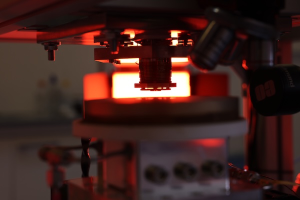
“ATLANT 3D builds materials and devices, atom by atom, through its direct atomic layer processing (DALP) technology, which places precise amounts of materials exactly where needed. In a single step, the system creates complex structures for microelectronics, semiconductors, and advanced devices. By replacing traditional multi-step fabrication with direct atomic-scale manufacturing, this approach eliminates process flow complexity while reducing material waste by at least 90 percent. Research teams use DALP technology to create what was previously impractical or impossible, from quantum computing components to devices that will operate in space.”
Challenges Faced
Have you faced any challenges in your sector of work recently? Dr. Plakhotnyuk acknowledged:
“Amidst cost-cutting initiatives like DOGE, the U.S. is pulling back on its financing of R&D. We view this as a big challenge, because at this stage, we are just starting to get known in the market. So against this backdrop, we need to gain trust from customers, validate use cases, and even choose market opportunities.”
Evolution Of The Company’s Technology
How has the company’s technology evolved since its launch? Dr. Plakhotnyuk noted:
“Quite a lot! We started by making the best micronozzle we could. Now we’re focused on meeting exacting industry standards geared towards delivering a new level of precise manufacturing and quality control, to ensure consistent performance. These include dimensional accuracy (with positional accuracy often within a micron); roundness of the orifice; aspect ratio (length to diameter), and more.”
Significant Milestones
What have been some of the company’s most significant milestones? Dr. Plakhotnyuk cited:
“We now support advanced packaging, referring to the integration of multiple semiconductor chips, components, and other devices into a single electronics package, instead of the traditional approach of packaging each chip individually. This technique allows for increased performance, reduced size and improved functionality, while accommodating Moore’s Law and the ever-pressing need for smaller, more powerful devices.”
Customer Success Stories
Can you share any specific customer success stories? Dr. Plakhotnyuk highlighted:
“In late 2023, ATLANT 3D announced a collaboration with the European Space Agency (ESA) to enable on-demand production of next-generation devices, microelectronics and more in space. The goal was to make on-demand repair, maintenance and manufacturing of high-precision components while in orbit possible, in the microgravity and zero gravity environment of space.”
“In March 2025 – about sixteen months later – ATLANT 3D and ESA announced they achieved a key milestone in their collaboration, a version of ATLANT 3D’s atomic layer deposition (ALD) system that can function in a real-world space deployment, called the Nanofabricator Zero-G System (zero G stands for “zero gravity”). Ultimately, this marks an important step towards fully autonomous deep space exploration and inhabitation, including the Moon and Mars.”
“In addition to our work with ESA, we have developed a number of processes with STMicroelectronics and other companies.”
Funding/Revenue
Are you able to discuss funding and/or revenue metrics? Dr. Plakhotnyuk revealed:
“In September 2022, we secured a $15 million funding round, led by West Hill Capital, Sony and other international investors. Shortly after securing this round, ATLANT 3D successfully launched Nanofabricator Lite as a product and a prototype of industrial multimodular Nanofabricator Flow. Nanofabricator Lite is a versatile system that uses DALP technology to accelerate materials and process research, device R&D, and prototype development. The University of Vermont became the first institution to acquire the system, marking a significant milestone. ATLANT 3D has since established partnerships with over 50 industrial and research organizations, including major semiconductor manufacturers like STMicroelectronics, Sony and several other Fortune 500 companies.”
“We also grew our team to more than 35 members, bringing in talent specializing in atomic layer deposition (ALD) and material sciences; filed for a total of 11 patents, with one granted in the U.S., Singapore, Japan, and South Korea; and expanded our validated materials library to a potential 20 materials. This allows for greater flexibility and innovation in developing new products and applications across various industries.”
“This initial funding round was followed by another $15M Series A+ round in March 2025, also led by West Hill Capital, further validating the excitement and momentum around our company.”
Total Addressable Market (TAM)
What total addressable market (TAM) size is the company pursuing? Dr. Plakhotnyuk assessed:
“We estimate the TAM size to be $1.59 trillion, with the serviceable addressable market (SAM) estimated at $500B and the serviceable obtainable market at $2.5B and to be expanded further.”
Differentiation From The Competition
What differentiates the company from its competition? Dr. Plakhotnyuk affirmed:
“As discussed above, our approach accelerates innovation across sectors by speeding up materials discovery while delivering a greener process. With global demand for semiconductors showing no signs of abating, the industry remains somewhat of a paradox. On the one hand, semiconductors are vital to cutting-edge eco-friendly developments like electric cars and environmental sensors. But on the other, the current impact of the manufacturing process on the environment, and the size of its ecological footprint, are untenable. Approaches like ATLANT 3D’s are designed to help resolve this conflict, once and for all.”
Future Company Goals
What are some of the company’s future company goals? Dr. Plakhotnyuk emphasized:
“With the Series A+ funding, ATLANT 3D plans to continue focusing on technology leadership and industrial product development, extending its global innovation network, broadening its application portfolio and strategic partnerships, and expanding its sales and marketing teams and commercial growth.”
Additional Thoughts
Any other topics you would like to discuss? Dr. Plakhotnyuk concluded:
“Another one of our strategic differentiators worth calling out is the fact that we offer a platform for natural resilience. Since President Trump highlighted the need for a robust domestic semiconductor manufacturing ecosystem during his first term, there have been more than 100 new semiconductor projects announced across 28 U.S. states. The U.S. is now on track to triple its chip manufacturing capacity by 2032 and command a sizable share of the world’s advanced chip production.”
“But winning the chip race worldwide will not be easy, and the U.S. must continue to bolster domestic chip production and advance innovation. We’re on the precipice of a major revolution in semiconductor manufacturing being led by companies like ATLANT 3D.”
“ATLANT 3D’s approach supports more semiconductor manufacturing in the U.S. because it moves away from the model of heavily offshoring production to a small handful of multi-billion dollar foundries, to leveraging universities, startups and industrial R&D based domestically to dramatically accelerate discovery and the entire lab-to-fab process, while keeping costs in check. By creating a platform for U.S. strategic resilience, ATLANT 3D is helping to reduce our country’s dependency on foreign supply chains by offering a modular platform, supporting research, prototyping, and manufacturing in an agile and digital process platform. Universities, startups and industrial R&D firms across the U.S. can integrate our technology immediately into their existing architectures.”