

UNISERS is a semiconductor metrology and inspection company that develops wafer inspection tools and analytical instruments designed to detect and characterize nanometer-scale contaminants in the chip manufacturing process. By making invisible particles visible and identifiable, they help manufacturers catch defects early and improve production yields. Pulse 2.0 interviewed UNISERS CEO Chuck Milligan to learn more.
Chuck Milligan’s Background

Could you tell me more about your background? Milligan said:
UNISERS is a Zurich-based semiconductor technology company focused on advancing contamination control for high-volume manufacturing. The company was founded around a breakthrough optical particle analysis technology and has evolved from deep-tech research into a commercial-stage provider of HVM (High Volume Manufacturing) automated fab tools.
Our mission is to bring molecular-level particle classification directly into semiconductor production environments.
Formation Of The Company
How did the idea for the company come together? Milligan shared:
The idea originated from a fundamental gap in semiconductor manufacturing: The drive toward sub-3nm transistor nodes, which enables leading-edge fabs to keep up with Moore’s law and enable the significant chip performance increases needed going forward, means that contamination particles which were not a problem in previous transistor node generations are yield killers today. This problem will keep getting more painful and expensive. UNISERS’ patented surface enhancement technology has been developed specifically to detect and identify contamination which, due to extremely small size and varying topology, is invisible to current inspection tools. This brings us a tremendous and fast-growing market opportunity.
UNISERS developed a proprietary optical approach that enables particle classification at a molecular level — not only for traditional defect inspection and review, but also for liquid defectivity applications, which are increasingly critical in advanced-node manufacturing.
The company was built to industrialize this innovation and integrate it into high-volume fab workflows.
Core Products
What are the company’s core products and features? Milligan explained:
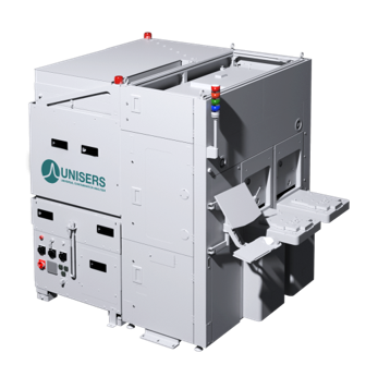
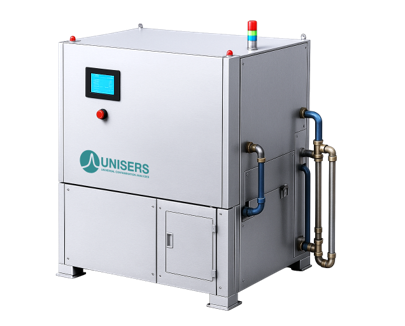
UNISERS offers automated fab-integrated high-volume manufacturing systems:
- Explorer – focused on advanced defect inspection and review, enabling detailed particle characterization.
- Inspector – designed for liquid defectivity applications, bringing molecular classification into liquid contamination control. (semi-automated system available, automated system launch in 2027)
Our systems combine proprietary coating technology and optical analysis to deliver:
- Sensitivity down to sub-10nm
- Rapid molecular particle classification
- Integration into existing high-volume manufacturing production workflows
This enables actionable contamination insight directly within manufacturing environments.
Differentiation From The Competition
What differentiates the company from its competition? Milligan affirmed:
Traditional systems primarily detect and count particles, but only at larger sites and in certain wafer substrate conditions. UNISERS enables fabs to see what is invisible today and provides fast molecular-level classification with sensitivity down to sub-10nm, suitable for high-volume manufacturing.
This allows semiconductor fabs not only to detect contamination events but to quickly understand material composition and implement targeted corrective actions.
Our proprietary coating process, optical stack, and integrated software platform create a defensible and differentiated solution designed for production-scale deployment.
Significant Milestones
What have been some of the company’s most significant milestones? Milligan cited:
- Granting of multiple patent families protecting our core technology
- Shipment in December 2025 and April 2026 of our first two fully automated fab tools to a leading-edge high-volume manufacturing customer
- Placement of a lab system at ITRI in Taiwan, a globally recognized semiconductor research institute
- Recent PO for a lab system from a leading chemical supplier in Taiwan
- We have been selected as a key participant the sub-10nm particle project from imec, the world’s leading independent nanoelectronics R&D hub
- Appointment of Chuck Milligan as CEO and Oreste Donzella, former C-suite executive at KLA, as incoming Chairman of the Board, strengthening industrial leadership
Customer Success Stories
Can you share any specific customer success stories? Milligan highlighted:
While detailed data remains confidential, we delivered a lab system to a leading-edge semiconductor manufacturer in 2024 to validate the technology in production-relevant use cases. Following successful validation, we shipped our first two fully automated fab tools to this customer in December 2025 and April 2026, marking the transition from lab evaluation to high-volume manufacturing deployment.
Challenges Faced
Have you faced any challenges in your sector recently? Milligan acknowledged:
Industrializing breakthrough technology for semiconductor fabs requires meeting stringent reliability, automation, and throughput requirements. Our focus has been on bridging deep scientific innovation with robust engineering, ensuring our systems meet the standards required for high-volume manufacturing environments.
Evolution Of The Company’s Technology
How has the company’s technology evolved since launching? Milligan noted:
The technology evolved from laboratory-based proof-of-concept systems into automated tools designed for fab integration. We significantly enhanced robustness, throughput, software-driven classification speed, and integration capabilities to support defect review and liquid defectivity use cases in production.
Total Addressable Market (TAM)
What total addressable market (TAM) size is the company pursuing? Milligan assessed:
UNISERS operates within the semiconductor process control and contamination management market, representing a multi-billion-dollar global opportunity. As chip node sizes shrink and manufacturing complexity increases, sensitivity to both particle and liquid contamination rises — expanding demand for advanced inspection and classification technologies in high-volume manufacturing.
Future Company Goals
What are some of the company’s future goals? Milligan emphasized:
Our focus is on scaling global deployment of our automated systems across the semiconductor ecosystem. We are advancing the launch and industrialization of our automated Inspector platform for liquid defectivity, while continuing to expand defect inspection and review applications. Our goal is to establish UNISERS as a scalable, high-volume manufacturing solution across multiple segments of semiconductor production worldwide.
Additional Thoughts
Any other topics you would like to discuss? Milligan concluded:
Contamination control is becoming increasingly critical as semiconductor processes reach atomic-scale dimensions. Technologies that combine ultra-high sensitivity with rapid classification in production environments will play a defining role in future yield optimization.
